
HDI circuit board, also known as high-density interconnect circuit board, is a newly emerging PCB manufacturing technology in the past decade. It mainly uses blind and buried hole technology to achieve high-speed signals and more precise circuits. Generally, it is rarely used in the non communication industry. In the past five years, with the demand for more precise chip design and packaging, more and more products need to be wired through HDI circuit boards to meet the functional requirements of the product. Today, vongsun will take you to understand the conventional stacked structure of one level HDI.
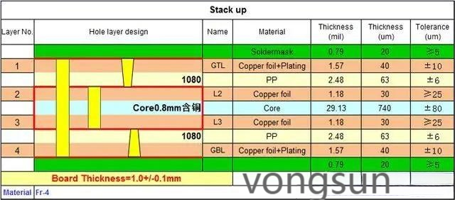
Structure of 4layers 1 level HDI(1+2+1)
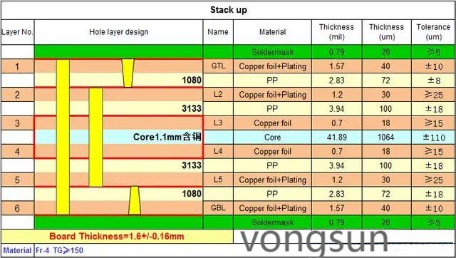
Stack-up Structure of 6layers 1 level HDI(1+4+1)
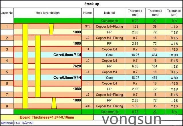
Stack-up Structure of 8layers 1 level HDI(1+6+1)
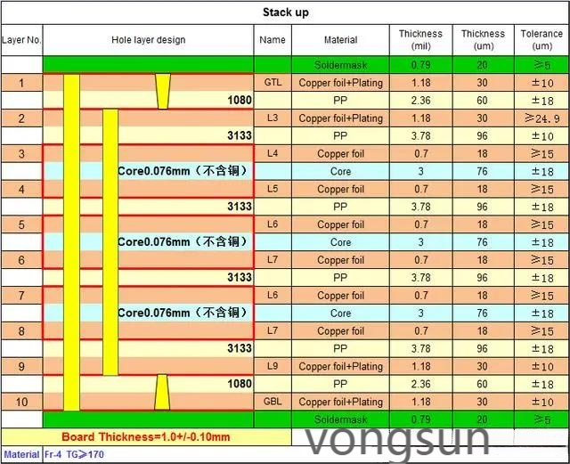
Stack-up Structure of 10layers 1 level HDI(1+8+1)
Contact us now to Learn more about the technical and professional knowledge of HDI circuit boards !!
Emails : sales@vongsun.com or sales@xsjcircuits.com