
PCB inspection, also known as PCB testing, is an extremely important production step in the production process of PCB circuit boards and an essential production process flow.
The purpose of PCB testing is to verify the rationality of PCB design and test for potential production defects that may occur during the PCB production process. Ensure the integrity of the product
Performance and availability. Improve product yield.
We can generally divide PCB inspection into two categories: manual visual inspection and inspection using instruments and equipment.
By visual inspection, we can check the appearance of the board, solder pads, solder mask ink, and the routing of the outer circuit for defects, which is relatively simple and direct Inspection method. But the efficiency is low and the reliability is low.The limitations of manual inspection are self-evident, and the use of advanced machinery and equipment can greatly improve the efficiency and reliability of detection.
Let's focus on the detection methods of common machines
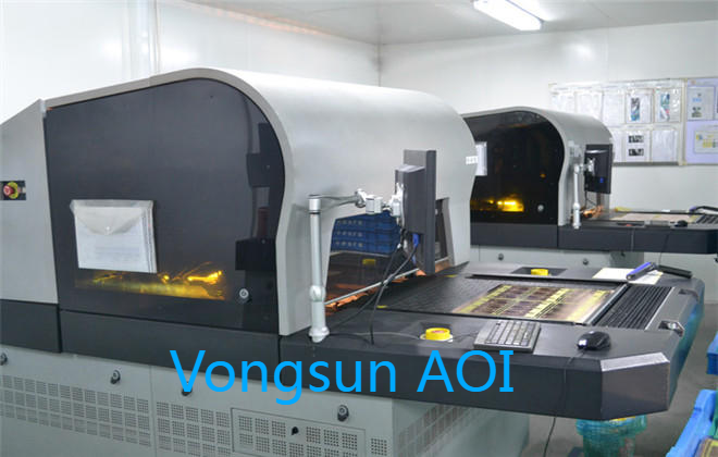
1.AOI
AOI usually uses the camera on the device to automatically scan the circuit board, in order to test the quality of the board. AOI devices may seem high-end, atmospheric, and upscale, but their flaws are also very obvious. It usually cannot recognize defects under bundles.
2.AXI
Automatic X-ray detection (AXI) is mainly used to detect the inner circuit of PCBs and is mainly used for testing high and multi-layer PCB circuit boards.
3.Flying probe
It uses probes on the device to test from one point on the circuit board to another when ICT power is needed (hence the name "flying needle"). Due to not being able to Customized fixtures are required, which can be used for testing scenarios of PCB fast boards and small to medium batch circuit boards.
4.Aging test
Usually, by powering on a PCB and conducting extreme aging tests in extremely harsh environments as permitted by the design, to see if it can meet the design requirements . Aging testing generally takes 48 to 168 hours.
5.X-ray testing
X-ray can detect the connectivity of the circuit, whether there are bulges and scratches on the inner and outer layers of the circuit. X-ray testing includes 2D and 3D AXI testing, and the testing efficiency of 3D AXI will be higher.
6.Function testing
Usually simulate the operating environment of the tested product and complete it as the final step before final manufacturing. The relevant test parameters are usually provided by the customer and may depend on the final use of the PCB. Usually, the computer is connected to a testing point to determine whether the PCB product meets its expected capacity.
In addition to the above testing methods, a PCB may also need to undergo the following tests
PCB contamination test: used to detect possible conductive ions on the board
Solderability test: used to check the durability of the board surface and the quality of solder joints
Microscopic section analysis: Slice the board to analyze the causes of problems that may occur on the board
Peel test: used to analyze the board peeled off from the board to test the strength of the circuit board
Float soldering test: Determine the thermal stress level of PCB holes during SMT surface mount soldering
Other testing processes can be synchronized with ICT or flying needle testing processes to better ensure the quality of the circuit board or improve testing efficiency.
We generally determine the use of one or several test combinations for PCB testing based on the requirements of PCB design, usage environment, usage, and production cost to improve product quality and reliability.
Vongsun is the high precision pcb manufaturer, We have high-precision production and testing equipment and a complete product quality control system. Highly favored by domestic and international customers.
1n