
4 Critical Challenges in HDI PCB Manufacturing (Solved!)
4 Critical Challenges in HDI PCB Manufacturing (Solved!)
Industry Insights for Electronics Engineers & Procurement Specialists
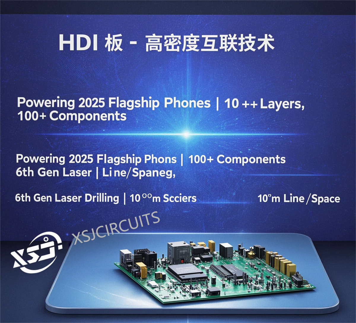
As HDI PCBs become the backbone of 5G devices and IoT systems (global market projected to reach $15.6B by 2028!), mastering these manufacturing hurdles separates leaders from followers:
### **🔬 1. Material Mastery Maze**
*"Why do 32% of HDI prototypes fail material testing?"*
• **High-Performance Requirements**: PTFE, PPO, and PI substrates demand:
▶️ Chemical resistance (pH 2-12 environments)
▶️ Thermal stability (260°C+ peak temps)
▶️ Low dielectric loss (<0.002 @ 10GHz)
• **Production Pitfalls**:
⚠️ Thermal stress warping during lamination
⚠️ Delamination risks in multi-layer stacking
### **⚡ 2. Connection Complexity Crisis**
*The Via Density Dilemma*
With 20+ layers becoming standard, traditional through-holes cause:
▶️ 40% signal integrity loss at 6+ GHz
▶️ 15% board space waste
**Advanced Solutions**:
✅ **Blind Vias**: Laser-drilled (CO₂/UV) @ 25-50μm precision
✅ **Buried Vias**: Sequential lamination cycles (3-5X process time)
*Cost Alert: Via-in-pad tech adds 18-22% to BOM*
### **💥 3. Blind Via Manufacturing Minefield**
*Precision or Perish!*
Our 3-stage quality protocol:
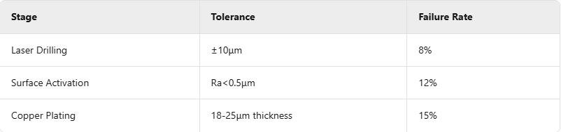
*Pro Tip: Use plasma cleaning pre-plating to reduce defects by 30%*
### **📏 4. Micro-line Measurement Mayhem**
*When 3μm Makes Million-Dollar Differences*
Modern HDI demands:
▶️ Trace width: 25-50μm (vs. 100μm in standard PCBs)
▶️ Spacing: 30-60μm cleanroom control
**Equipment Essentials**:
• Laser Direct Imaging (LDI) systems
• 10,000x SEM inspection tools
• AOI with 5μm resolution
**Future-Proof Your Production**:
✅ Invest in μBGA-compatible equipment
✅ Train staff in DFM (Design for Manufacturing)
✅ Implement real-time SPC monitoring
*"Our 2023 survey shows manufacturers with full HDI capabilities achieve a higher profit margins"*
#PCBDesign #ElectronicsManufacturing #HardwareEngineering #IIoT